How it works
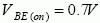
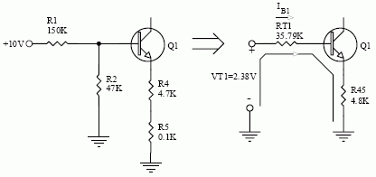
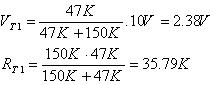
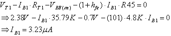
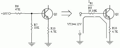
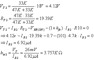
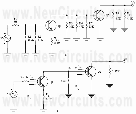
Begin with the DC operating point. At steady state, coupling capacitors block DC, so the bias networks can be analyzed independently. Replace each bias divider by its Thevenin equivalent, then solve for transistor currents and voltages using the stated model assumptions.
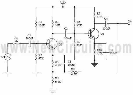
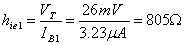
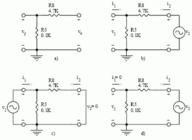
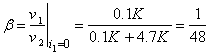
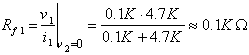
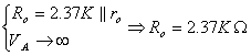
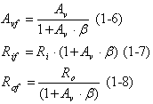
Next build the small-signal equivalent. Include the feedback network’s loading rather than treating it as an ideal voltage sampler. Calculate the forward behavior and feedback relationship using a consistent definition of loop gain.
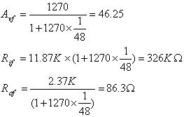
Finally compare the predicted input impedance, output impedance, and closed-loop gain with a simulation or measurement. Agreement depends on transistor parameters, bias point, frequency, and capacitor behavior.
Original archive figures
CLICK TO ENLARGEOn the bench
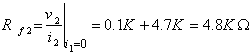
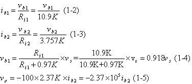
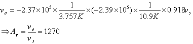
The original equation and analysis figures are preserved below. They are archival material; the typeset derivation and numerical results still require a dedicated technical review.
Resources & provenance
Rewritten from the original articles/ael/d3mn6sf_ael001.php page. Component values and historical performance claims have not been independently bench-tested.
Browse all surviving downloads →