How it works
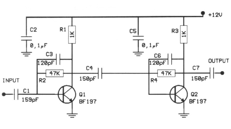
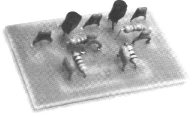
Each transistor stage uses resistive biasing and capacitive coupling. Cascading two stages increases overall gain while the transistor and layout determine the usable frequency range. The original project proposes BF197 devices and a regulated 12 V supply.
The original claims approximately 20 dB total gain and response extending toward 500 MHz. These are unverified design claims; high-frequency layout, actual device gain, and the connected source and load can change the result substantially.
Original archive figures
CLICK TO ENLARGEOn the bench
Keep lead lengths short and fit the finished board in a grounded metal enclosure. Check stability and gain over the intended band before using it ahead of a receiver.
Resources & provenance
Rewritten from the original projects/sub/d3mn6sf_prjsub003.php page. Component values and historical performance claims have not been independently bench-tested.
Browse all surviving downloads →